Although I did have some ideas on how to improve the performance of the current I/O circuit, it was already faster than I could measure so I had no way to know if my improvements were actually making it any better. Ideally I'd just buy an oscilloscope with several GHz of bandwidth, but I'm not made of money and those scopes tend to be in the "request a quote" price range.
The obvious solution was to build one. I already had a proven high-speed sampling architecture from my TDR project so all I had to do was repackage it as an oscilloscope and make it faster still.
The circuit was beautifully simple: an output from the FPGA drives a 50 ohm trace to a SMA connector, then a second SMA connector drives the positive input of an ADCMP572 through a 3 dB attenuator (to keep my signal within range). The negative input is driven by a cheap 12-bit I2C DAC. The comparator output is then converted from CML to LVDS and fed to the host FPGA board. Finally, a 3.3V CML output from the FPGA drives the latch enable input on the comparator.
The "ADC" algorithm is essentially the same as on my TDR. I like to think of it as an equivalent-time version of a flash ADC: rather than 256 comparators digitizing the signal once, I digitize the signal 256 times with one comparator (and of course 256 different reference voltages). The post-processing to turn the comparator outputs into 8-bit ADC codes is the same.
Unlike the TDR, however, I also do equivalent-time sampling in the time domain. The FPGA generates the sampling and PRBS clocks with different PLL outputs (at 250 MHz / 4 ns period), and sweeps the relative phase in 100 ps steps to produce an effective resolution of 10 Gsps / 100 ps timebase.
Without further ado here's a picture of the board. Total BOM cost including connectors and PCB was approximately $50.
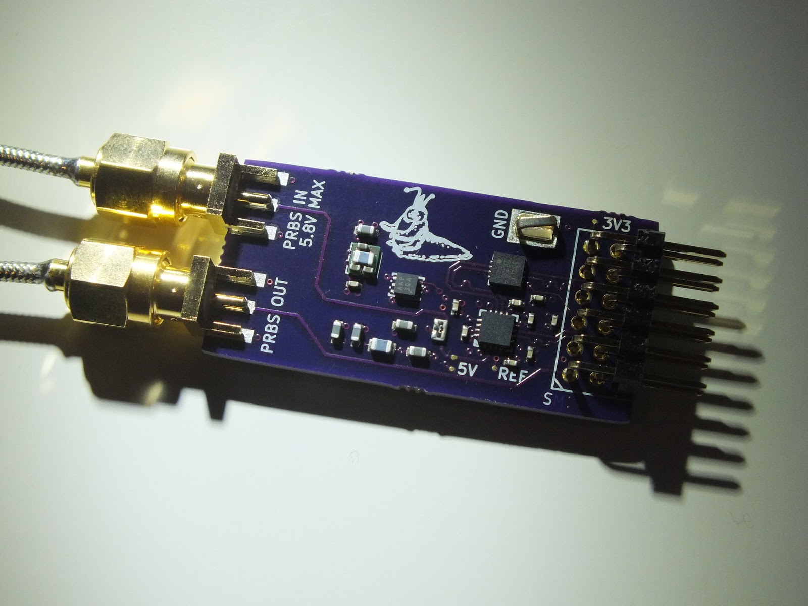 |
| Oscilloscope board (yes, it's PMOD form factor!) |
 |
| 250 Mbps: very bumpy rise |
 |
| 500 Mbps: significant eye closure even with increased drive strength |
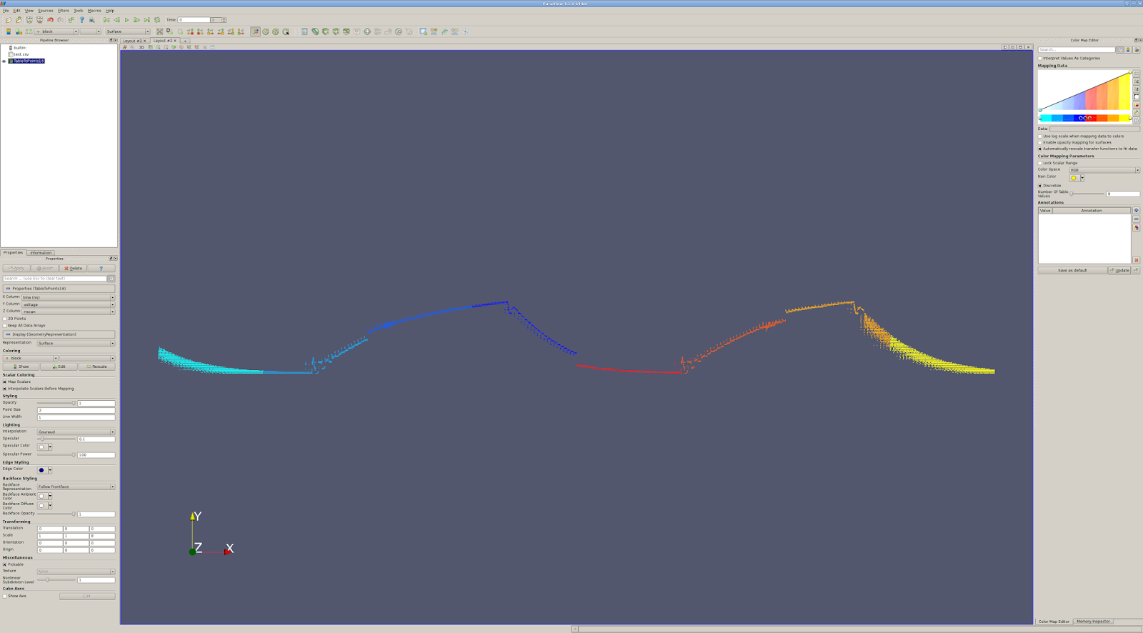
I spent quite a while tracking down other bugs before dealing with the signal integrity issues. For example, a low-frequency pulse train showed up with a very uneven duty cycle:
 |
| Duty cycle distortion |
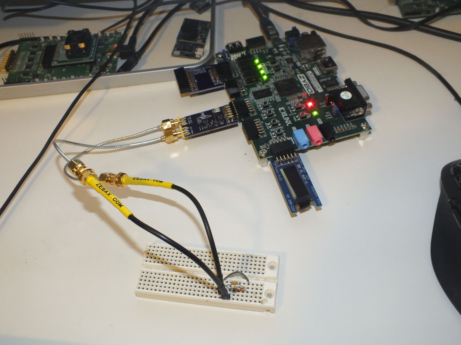 |
| Ever seen breadboarded passives interfacing to edge-launch SMA connectors before? |
 |
| I don't have an EE degree, but I can tell this looks wrong! |
Interestingly enough, two blocks (of 32 samples each) were concatenated into a single JTAG transfer. These two were read in one clock cycle and looked fine, but the junction to the next transfer seemed to be skipping samples.
As it turned out, I had forgotten to clear a flag which led to me reading the waveform data before it was done capturing. Since the circular buffer was rotating in between packets, some samples never got sent.
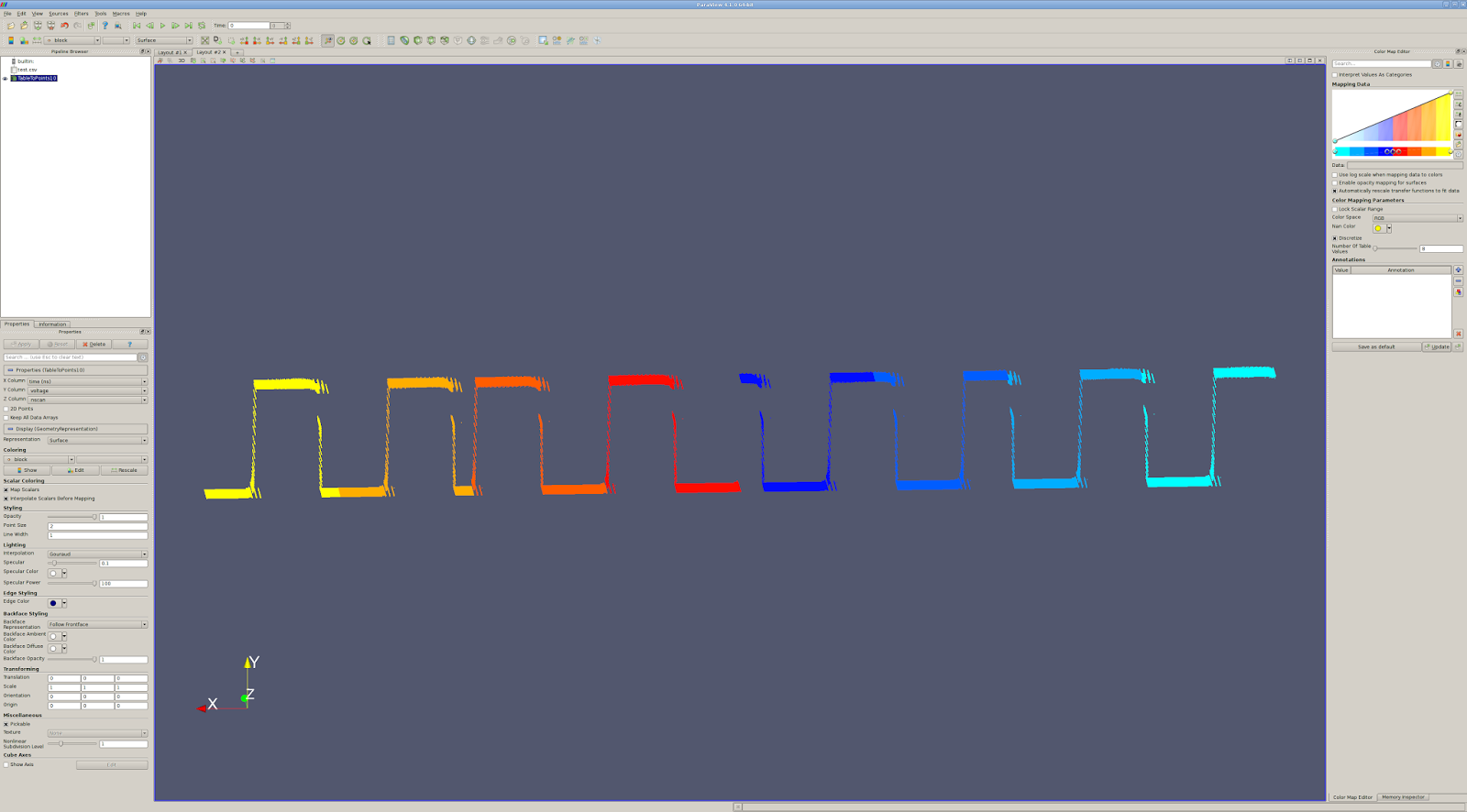
The next bug required zooming into the waveform a bit to see. The samples captured on the first few (the number seemed to vary across bitstream builds) of my 40 clock phases were showing up shifted by 4 ns (one capture clock).
 |
| Horizontally offset samples |
I traced this issue to a synchronizer between clock domains having variable latency depending on the phase offset of the source and destination clocks. This is an inherent issue in clock domain crossing, so I think I'm just going to have to calibrate it out somehow. For the short term I'm manually measuring the number of offset phases each time I recompile the FPGA image, and then correcting the data in post-processing.
The final issue was a hardware bug. I was terminating the incoming signal with a 50Ω resistor to ground. Although this had good AC performance, at DC the current drawn from a high-level input was quite significant (66 mA at 3.3V). Since my I/O pins can't drive this much, the line was dragged down.
I decided to rework the input termination to replace the 50Ω terminator with split 100Ω resistors to 3.3V and ground. This should have about half the DC current draw, and is Thevenin equivalent to a 50Ω terminator to 1.65V. As a bonus, the mid-level termination will also allow me to AC-couple the incoming signal if that becomes necessary.
 |
| Mill out trace from ground via to on-die 50Ω termination resistor |
 |
| Remove soldermask from ground via and signal trace |
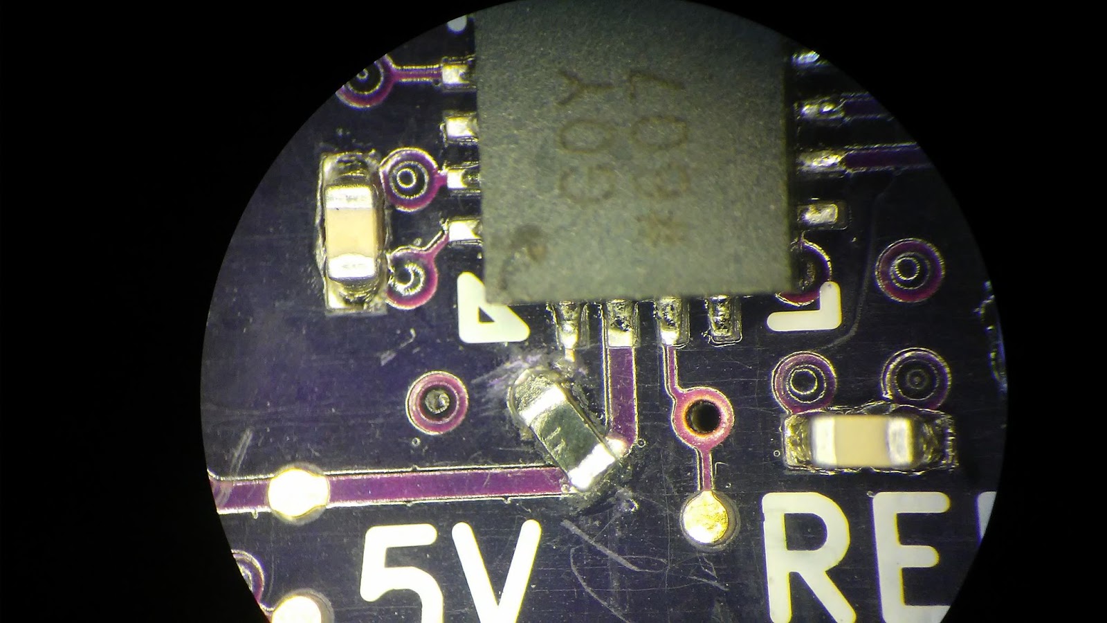 |
| Add 100Ω 0402 low-side terminator |
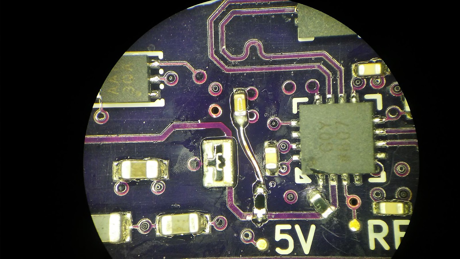 |
| Add 100Ω 0402 high-side terminator, plus jumper trace to 3.3V bulk decoupling cap |
 |
| Add 10 nF high speed decoupling cap to help compensate for inductance of long feeder trace |
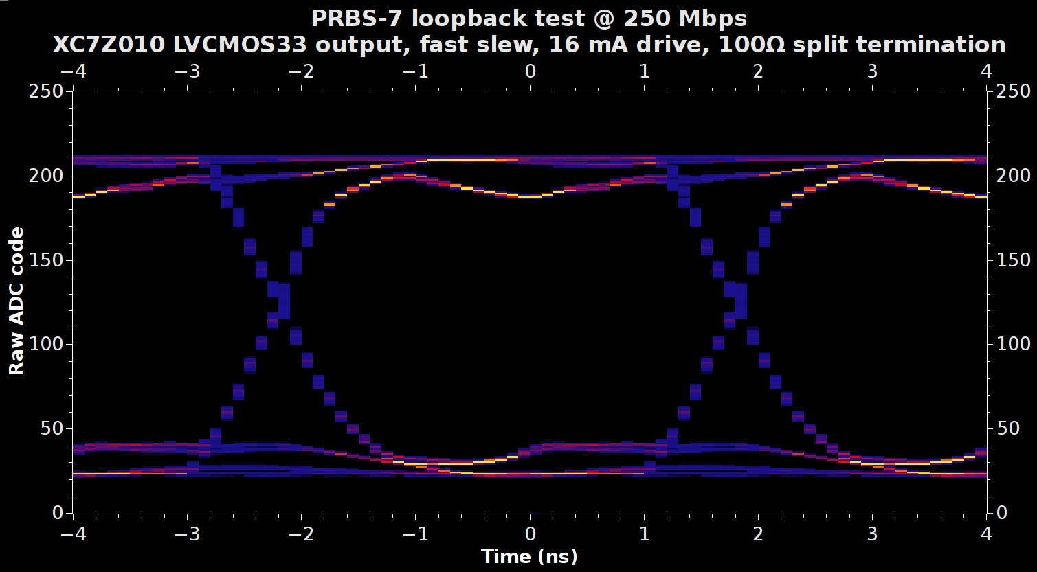 |
| Post-rework at 250 Mbps |
 |
| Post-rework at 500 Mbps |
Next step: collect some baseline data for the current STARSHIPRAIDER characterization board, then use that to inform my v0.2 I/O circuit!
This is impressive stuff. Any tips on how I could get high bandwidth, i.e. >1Gb/s signal from a Pmod connector? Or just in general out of one of these pynq or zedboard FPGA boards?
ReplyDelete